Semiconductor wafer and printed-circuit-board (PCB) production lines now rely on ultra-high-resolution imaging to catch defects that shrink below 5 µm. Vision engineers entering this space often ask which sensor resolution, which data interface, and which system topology will future-proof their inspection tools. The following expert Q&A addresses the three most common questions using real-world performance data taken directly from KAYA Vision’s latest camera and frame-grabber portfolio.
Which camera offers 100 MP class performance for electronics inspection?
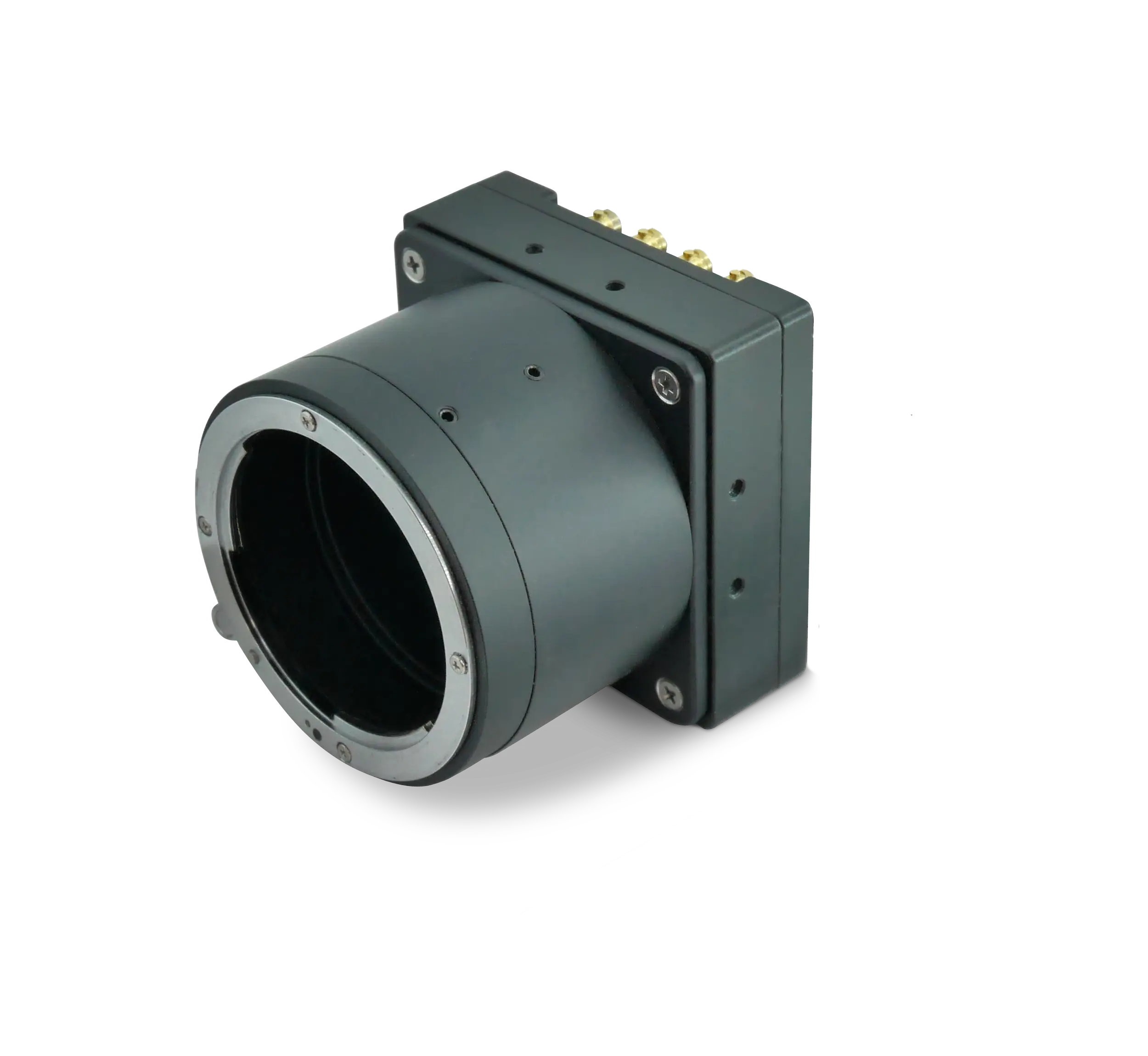
When an inspection station calls for roughly 100 megapixels or more, engineers frequently choose the Zinc 661 PCIe. Powered by Sony’s 3.45 µm global-shutter IMX661, the Zinc 661 records 13 400 × 9 528 pixels—about 128 MP per frame—delivering true sub-3 µm spatial sampling when paired with 10× telecentric optics on 300 mm wafers. This oversampling exceeds the 5 µm critical-defect guideline in the IPC-A-610G standard, enabling reliable automated optical inspection (AOI) of solder joints, micro-vias, and lithography patterns without resorting to multiple passes.
The camera streams images over an eight-lane PCI Express Gen 3 interface. An x8 Gen 3 link supplies up to 6.7 GB/s of effective host bandwidth, so no separate frame grabber is required. The Zinc 661 maintains 21.5 fps at 8- or 10-bit output, 19.6 fps at 12-bit, and 12.9 fps at 14-bit—speeds fast enough for step-and-scan wafer stages or high-throughput inline PCB conveyors. A measured dynamic range above 70.8 dB captures glossy aluminum pads and dark photoresist in the same exposure, while temporal noise stays below 2.7 e- to preserve signal integrity for subtraction or AI-based enhancement.
Cleanroom integrators appreciate several mechanical touches. Active sensor alignment keeps each corner of the 56.7 mm-diagonal sensor in focus, and an optional IP67 lens tube protects the optical path from flux residues or dicing-saw mist. Both monochrome and color variants are available: monochrome for solder-mask or bump-height metrology, color for component presence or label verification. GenICam-compliant control means existing semiconductor tools that already support GenICam can add the Zinc 661 with minimal user-interface rework.
Is CoaXPress the best choice for multi-gigapixel inspection lines?
Yes—especially when several ultra-high-resolution camera heads must be synchronized and their aggregate data stream exceeds 25 Gb/s. KAYA Vision’s Iron 4600 transmits up to 100 fps at 8-bit through four CXP-12 lanes. On the host side, the Komodo III Quad CoaXPress 12G Frame Grabber ingests as much as 50 Gb/s from one to four cameras and DMA-transfers the image buffers into host RAM or GPU memory at a sustained 6.7 GB/s.
This topology avoids cable-length and peer-to-peer limitations. Micro-BNC coax rated for CXP-12 can span roughly 40 m, so you can isolate vibration-sensitive optics from EMI-noisy power cabinets without resorting to fiber repeaters. Power over CoaXPress (PoCXP) delivers up to 13 W per connector, eliminating separate power harnesses inside fast-moving gantry scanners and easing cable-chain design.
For builders targeting multi-gigapixel stitching—imagine six Iron 4600 color cameras tiled over a 610 × 610 mm server board—the Komodo III’s 4 GB of onboard DDR4 memory soaks up encoder-driven burst triggers without dropping frames. The board provides on-the-fly 16-bit Bayer demosaic, color-space conversion, and an 8 ns-resolution timestamp, giving deterministic latency that closed-loop systems rely on when AOI feedback must adjust pick-and-place heads or laser trimmers in real time.
The Iron 4600 itself pairs a 4.4 µm pixel with a 43.8 mm-diagonal sensor. Although its rolling-shutter architecture may look unfamiliar to teams used to global-shutter devices, the 2.5 µs minimum exposure and sub-1.6 e- temporal noise still capture fast-moving panels sharply under proper strobe illumination. A dynamic range greater than 90 dB at 520 nm keeps copper pours and high-contrast silkscreen within the 14-bit output so downstream classification networks are not forced to choose between clipping and under-exposure.
Do higher megapixels really improve PCB defect detection?
In most AOI tasks the answer is a clear yes. Higher megapixels shrink the projected pixel size on the inspected surface, reducing modulation-transfer-function (MTF) loss introduced by optical demagnification. Upgrading from a legacy 20 MP camera to the 128 MP Zinc 661, for example, cuts the pixel footprint on a 50 mm-wide trace region from roughly 2.5 µm to about 0.5 µm without changing optics. Solder-ball voids or under-etch pits that once occupied a single ambiguous pixel now spread across five or more, boosting the confidence of AI classifiers beyond the 0.95 thresholds many IPC test plans demand.
Pixel count, however, is only one piece of the signal-integrity puzzle. Dynamic range, quantum efficiency, and noise floor determine whether faint discolorations or shallow dents emerge from background texture. The Iron 4600’s measured dynamic range above 90 dB captures both white silkscreen and copper pours in one shot; the Zinc 661’s >70.8 dB still outperforms many smaller-format imagers. Quantum efficiency exceeding 63 % (Zinc 661) and 84 % (Iron 4600) at 520 nm keeps exposure times short enough for high-speed conveyors, while low temporal noise maintains algorithmic stability when background subtraction or hybrid classical/AI pipelines are used.
Flexibility also matters. Both the Zinc 661 and Iron 4600 support region-of-interest (ROI) readout and on-camera binning. An integrator can zoom in to full 128 MP only when a machine-learning model flags a suspect die or fine-pitch ball-grid array, then fall back to a binned, lower-resolution mode for coarse screening, trading resolution for up to four times the sensitivity and markedly higher throughput. Because these modes are addressed through standard GenICam nodes, a scheduler running on the host PC can switch modes on the fly without proprietary SDK calls.
Of course, a sensor that generates hundreds of megapixels per frame needs a transport layer that keeps pace. A single uncompressed 128 MP, 12-bit frame weighs about 307 MB. At 20 fps that is more than 6 GB/s—within PCIe Gen 3 x8 limits but far beyond USB 3 or GigE Vision. Likewise, four Iron 4600 cameras streaming 85 fps at 10-bit each would produce nearly 18 GB/s of raw data, a load the Komodo III and its 50 Gb/s CXP back end are specifically built to handle. Choosing a high-bandwidth interface up front prevents costly rewiring when future product iterations require faster tact times or additional inspection angles.
Finally, system-level determinism cannot be overlooked. Jitter in trigger distribution, encoder decoding, or buffer allocation can blur the correlation between an image and the motion-stage coordinates reported to the factory MES. The Komodo III’s 64-bit, 8 ns-precision timestamping and quadrature-encoder inputs synchronize multiple cameras far more tightly than software timers or network-based handshakes. Meanwhile, both cameras’ opto-isolated I/O lines simplify galvanic isolation between sensitive image-sensor grounds and high-current motor drivers, reducing electromagnetic crosstalk that could otherwise degrade image quality.
In summary, higher megapixels absolutely improve defect detection—but only when combined with low-noise sensors, broad dynamic range, deterministic trigger pipelines, and the right data interface. KAYA Vision’s Zinc 661 PCIe delivers the raw resolution for sub-5 µm semiconductor and PCB inspection without the need for an external frame grabber. The Iron 4600, paired with the Komodo III Quad CoaXPress 12G frame grabber, scales that performance to multi-camera, multi-gigapixel systems while maintaining predictable latency and reliable power delivery. Together these products provide a coherent, standards-based ecosystem that lets inspection-tool designers meet today’s defect-density targets and still leave bandwidth headroom for tomorrow’s even finer process nodes.