Semiconductor fabrication lines live or die by sub-micron precision. A single defect on a 300 mm wafer can translate into millions in lost revenue, and modern process nodes demand not only optical quality but blazing throughput. Selecting the optimal high-resolution camera for semiconductor inspection therefore becomes a mission-critical engineering decision. This guide dives deep into the image sensor specifications, evaluation workflows, and system integration steps you should master when configuring wafer-inspection machine-vision cameras around KAYA Vision’s industrial high-megapixel portfolio.
Why Resolution and Pixel Size Matter
In back-end and front-end inspection, you fight two competing forces: resolving the smallest pattern defects and imaging an entire die (or multiple dies) fast enough to avoid bottlenecks. A larger sensor with more pixels allows you to capture a bigger field of view (FOV) at a given microscope objective while still hitting the critical sampling rate. KAYA Vision’s Zinc 661 PCIe delivers 134 MP on a 56.7 mm diagonal, enabling single-shot coverage of 12-inch wafers at roughly 1 µm per pixel when paired with telecentric optics. Smaller pixel sizes—3.45 µm in this case—also boost spatial resolution, but they must be balanced against diffraction limits and lens numerical aperture (NA) to maintain modulation transfer function (MTF).
If your toolset targets mid-die metrology rather than macro inspection, the 65 MP Iron 3265 with 3.2 µm pixels strikes an ideal equilibrium between sampling density and sensitivity. For patterned-wafer macro defect-review lines that value higher full-well capacity over sub-micron pitch, the 45 MP Iron 4600 and its 4.4 µm photosites supply generous 50 ke- electron wells, cutting shot noise when measuring low-contrast particles.
Global Versus Rolling Shutter
Most wafer handlers move substrates at high speed under the optics, so any skew between illumination and sensor readout can generate motion artifacts that mask yield-killing errors. The Zinc 661 PCIe and Iron 3265 use a true global shutter that exposes every pixel simultaneously, eliminating rolling-distortion risk and enabling strobed illumination techniques. The Iron 4600, by contrast, employs a high-speed rolling shutter; with its 2.5 µs minimum exposure it can still freeze many inspection motions, but you must validate that stage velocity and line-time do not exceed allowable blur.
Combine global-shutter sensors with programmable exposure control—down to 10 µs on the Zinc 661 PCIe—and you can freeze even the fastest indexer movements in bright-field or dark-field illumination schemes.
Dynamic Range and Defect Contrast
Bright-field and dark-field inspections create extreme contrast swings across polished silicon, copper interconnects, and photoresist features. An industrial high-megapixel camera must therefore sustain high dynamic range (HDR) without sacrificing speed. The Iron 4600 reaches >90 dB, allowing it to image specular die pads and dark trenches in a single frame. The Zinc 661 PCIe, with >70 dB and <2.7 e- temporal noise, still outperforms many legacy CCD solutions and benefits from on-sensor defect-pixel correction to guard against hot sites that could be misread as particles.
Frame Rate, Interface, and Throughput Calculations
Throughput targets are often expressed in wafers per hour (WPH). To translate that into camera specifications, perform an FOV calculation based on your objective magnification, then divide the total die area by the captured FOV to estimate image tiles per wafer. For example, imaging an entire 300 mm wafer at 10× with the Zinc 661 PCIe may require around 400 tiles. At 21.5 fps and PCIe Gen3 direct streaming into a GPU, you could theoretically acquire the whole wafer in under 20 seconds, excluding stage overhead.
The CoaXPress 2.1 interface on Iron cameras pushes comparable bandwidth through long coax cables with Power-over-CXP. The Iron 4600 sustains 100 fps at 8-bit; multiply by a 45 MP frame and you exceed 4 GB/s of raw data, more than enough for high-mix lines. If your automated-optical-inspection (AOI) tool is space-constrained, the 62 mm × 62 mm body of the Iron 3265 reduces enclosure footprint while still using four micro-BNC connectors for an aggregate 50 Gbps link.
Opto-Mechanical Alignment
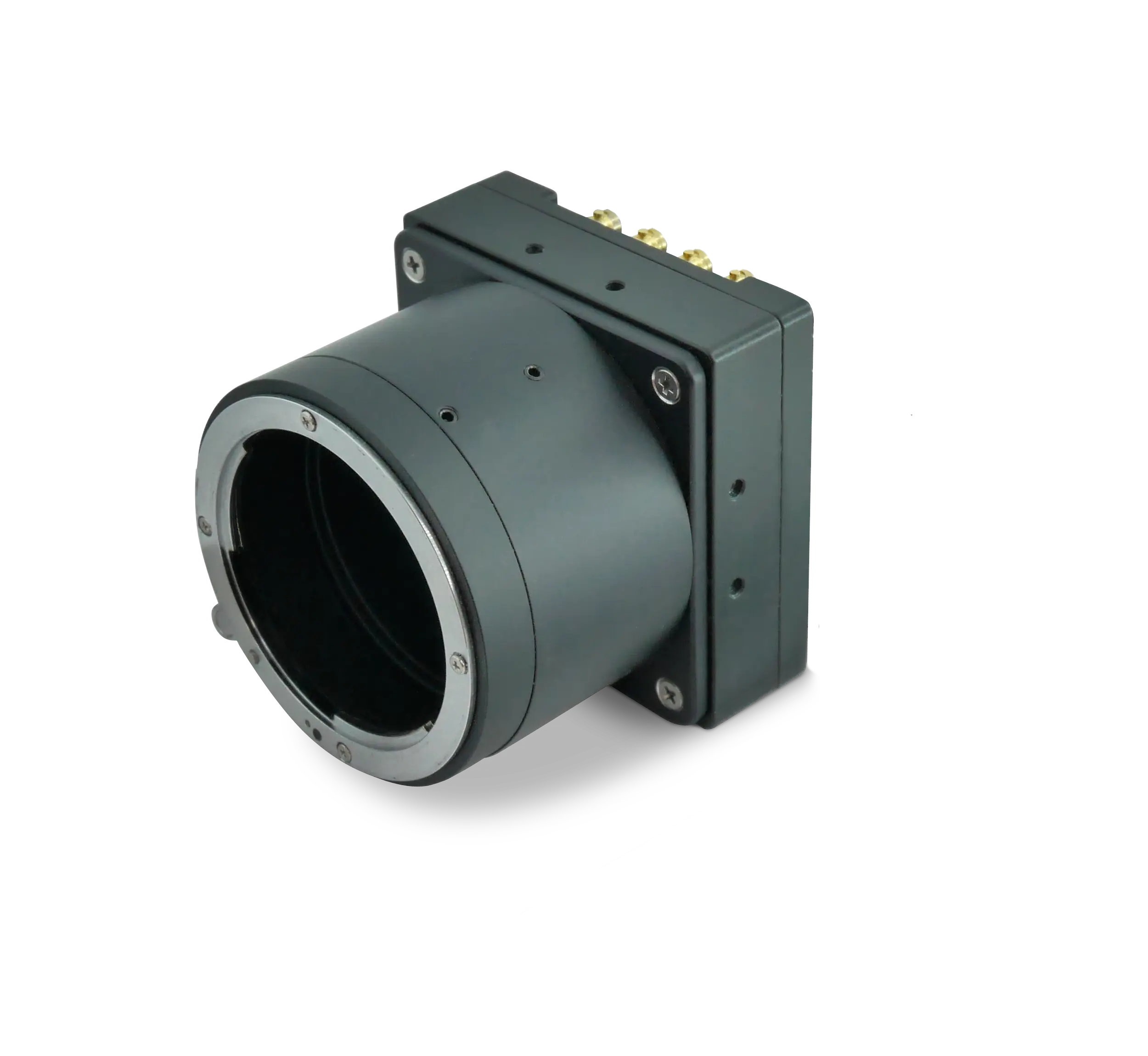
Inspection repeatability depends on sensor flatness relative to the lens mount. KAYA Vision performs active alignment on every high-resolution camera shipped for semiconductor inspection. The Iron 3265 guarantees ≤0.15° sensor orthogonality, while the Zinc 661 PCIe offers optional IP67 ingress protection and an M72 mount that keeps large-format objectives stable during 24/7 operation.
Controlling Illumination and Triggering
The programmable GPIO on each KAYA industrial high-megapixel camera simplifies synchronization with ring lights, laser strobes, and off-axis dark-field bars. Four general-purpose timers and counters inside the Zinc 661 PCIe can strobe exposure outputs with sub-microsecond precision, letting you time a 10 µs global exposure exactly between stepper-motor jerk events. For multi-camera mosaics across a future 450 mm-wafer roadmap, GenICam builds a deterministic trigger chain so every capture aligns to the same encoder tick.
Data Pipeline and AI Readiness
Modern inspection no longer ends at simple thresholding. Deep-learning models analyze gigapixel wafer images for systematic patterning defects. That means feeding GPUs or edge TPUs with data as little compressed as possible. Direct PCIe-Gen3 streaming on the Zinc 661 PCIe offers zero-copy transfer into host memory, avoiding the overhead associated with external frame-grabber DMA. CoaXPress 2.1 cameras like the Iron 3265 integrate smoothly with KAYA’s four-lane frame grabbers where FPGA preprocessing—binning, ROI cropping, LUT-based contrast expansion—can cut data volume before the neural network sees a single tensor.
KAYA Vision Model Selection Cheat-Sheet
- Zinc 661 PCIe (134 MP, global shutter): Macro/global wafer review, photomask inspection, ultra-wide-FOV mappings demanding the highest resolution.
- Iron 3265 (65 MP, global shutter): Reticle alignment, die-level defect classification, AI pipelines where 31–71 fps suffices.
- Iron 4600 (45 MP, rolling shutter, 100 fps): High-dynamic-range metal-layer inspection and bump inspection requiring fast cycle time with robust PoCXP single-cable deployment.
Deploying the correct wafer-inspection camera therefore hinges on a systematic breakdown of optical, electronic, and mechanical parameters. By aligning critical-dimension targets, throughput budgets, and data-infrastructure limits with the strengths of KAYA Vision’s Zinc and Iron families, engineers can implement inspection platforms that catch sub-micron defects while still driving fab cycle time forward.